MNE 2026 will open with a dedicated tutorial programme on Monday, 21 September 2026. The programme includes two half-day tutorials and one full-day tutorial featuring leading experts from academia and research.
Registration information:
- Participants may choose to participate at T1 + T2 OR T3.
- Coffee breaks, snacks and a light lunch is included with the tutorial registration fee.
- Tutorials are open to MNE 2026 delegates only as an ADD-ON option to conference registration.
Tutorial Fees
| EARLYBIRD Until July 24 | REGULAR July 25 - September 18 |
|
|---|---|---|
| 8.1% VAT included in all rates. All fees in Swiss Franc (CHF) | ||
| TUTORIALS - STANDARD | 160 | 190 |
| TUTORIALS - STUDENT | 110 | 135 |
- Tutorial 1 (T1) – Optical metasurfaces and metalenses
- Tutorial 2 (T2) – Bioiontronics for biointerfaces and future medicine
- Tutorial 3 (T3) – Sustainable semiconductor manufacturing & life cycle assessment
Tutorial 1 · 09:30–12:30
Location: MNE 2026 Venue, room to be determined
Optical metasurfaces and metalenses: design, materials, manufacturing and applications
Abstract: This tutorial will cover the basic principles of optical metasurfaces and metalenses, which are promising disruptive optical elements. The design process, and methodologies how to realize them with nanofabrication and related materials. They will be introduced by giving examples of various applications such as 3D depth sensor, LiDAR, camera, and extended reality glass.
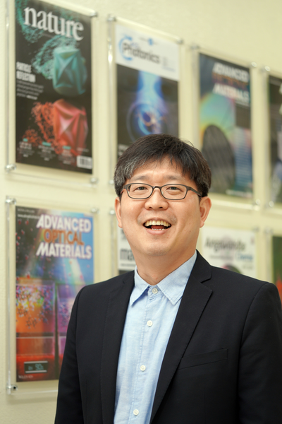
Biography: Junsuk Rho is a Yeon-San Endowed Chair Professor and Mu-Eun-Jae Endowed Chair Professor at Pohang University of Science and Technology (POSTECH), Korea, with a joint appointment in the Department of Chemical Engineering, Mechanical Engineering, and Electrical Engineering. He received his Ph.D. at the University of California, Berkeley (2013), M.S. at the University of Illinois, Urbana-Champaign (2008) and B.S. at Seoul National University, Korea (2007) all in Mechanical Engineering. Prior to joining POSTECH, he conducted postdoctoral research in Materials Sciences Division & Molecular Foundry at Lawrence Berkeley National Laboratory, and also worked as a principal investigator (Ugo Fano Fellow) in Nanoscience and Technology Division & the Center for Nanoscale Materials at Argonne National Laboratory. Prof. Rho has authored and co-authored more than 450 high-impact journal papers including Science and Nature. He is also the recipient of several notable honors and awards such as US Department of Energy Argonne Named fellowship (2014), Korean Presidential Early Career Award for Scientists and Engineers (2019), Member of the Young Korean Academy of Science and Technology (Y-KAST) (2020), Associate Member of the National Academy of Engineering of Korea (NAEK) (2022), Fulbright Visiting Scholar Fellowship (2022), Northwestern Simpson Fellowship (2022), Clarivate Highly Cited Researcher (2023, 2024), Elsevier/Stanford World Top 2% Scientist (2021-2025), and ACS Nano Lectureship (2024). He serves 13 editorial positions including Light: Science and Applications, Microsystems and Nanoengineering, and npj Nanophotonics.
Tutorial 2 · 13:15–15:30
Location: MNE 2026 Venue, room to be determined
Bioiontronics for biointerfaces and future medicine
Abstract: Bioiontronics is an important interdisciplinary field emerging from a confluence of recent breakthroughs in iontronics and bioengineering. The fundamental task of bioiontronics is to promote communication with living matter through ions and biological molecules and thereby mediate the detection and modulation of biological activities. Bioiontronics can function at abiotic-biotic interfaces in an autonomous fashion or in integral, modular components of biomedical devices. In this Tutorial, I will discuss the underlying mechanisms of bioiontronic devices and describe the challenges in their fabrication and application. I will then highlight recent prototypes and breakthroughs in bioiontronics and envision the future of the field. Elevation of bioiontronics through a union of multidisciplinary skills will disrupt the medical landscape and stimulate opportunities in areas such as soft robotics and neuromorphic computing.
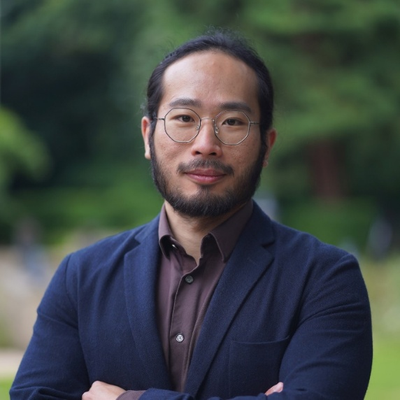
Biography: Yujia Zhang is an Assistant Professor of Electrical and Microengineering at the Institute of Electrical and Microengineering at EPFL. His research thrusts include iontronic hybrid tissues and wearable/implantable bioelectronics for applications in biomedicine. Recently, he has pioneered the area of dropletronics, in which networks of microscale soft droplets function as versatile bioelectronic/bioiontronic devices. Prior to his appointment, he obtained his B.Sc. in Electronics and Information Science and Technology from the University of Science and Technology of China in 2016. Later, he completed his PhD in biomedical engineering and MEMS/NEMS technology at the Shanghai Institute of Microsystem and Information Technology, Chinese Academy of Sciences, followed by one year as a visiting scholar at Stony Brook University, USA. In 2021, Yujia joined the Bayley group at the University of Oxford, UK, and started his postdoctoral research focusing on the development of multifunctional iontronic synthetic tissues for biotic interfaces and soft implants. In 2023, he became an independent early-career research fellow hosted in the Department of Chemistry at the University of Oxford.
Tutorial 3 · 09:30–16:30
Location: MNE 2026 Venue, room to be determined
Towards Sustainable Semiconductor Manufacturing & Life Cycle Assessment in Microelectronics (from clean room to components & systems)
This full-day tutorial addresses sustainability challenges and opportunities across semiconductor manufacturing, microelectronics production, and cleanroom operations, with contributions from experts working on environmental assessment, resilience, and life cycle analysis.
- Isabelle Servin – Sustainable process strategies based on the environmental footprint of semiconductor manufacturing
- Yannick Rivoira – From Silica Sand to Semiconductors: Understanding and Assessing Environmental Impacts in Cleanroom Manufacturing
- Sébastien Toussaint – Implementing resilience with ICTs
- Jeff Kettle – Life Cycle Analysis of electronic assemblies and discrete components to reduce environmental impact as well as waste
- Cyrille Hibert – EPFL-CMi cleanroom carbon footprint, including hotspot identification, opportunities for improvement, and the transformations already underway
Isabelle Servin
Lecture: Sustainable process strategies based on the environmental footprint of semiconductor manufacturing
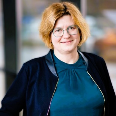
Biography: Isabelle SERVIN is a research scientist at CEA-Leti, Grenoble (France). She received her PhD on polymer chemistry from University Pierre & Marie Curie (Paris, France) in 1998. She is a research scientist at CEA-Leti with 20 years of experience in microelectronics lithography. Since 2022, she leads sustainability initiatives for cleanroom operations, managing EU programs and applying Life Cycle Assessment to reduce environmental impact in the IC industry. Her work bridges advanced semiconductor process development with sustainable innovation strategies to support the transition toward greener microelectronics.
Yannick Rivoira
Lecture: From Silica Sand to Semiconductors: Understanding and Assessing Environmental Impacts in Cleanroom Manufacturing
Biography: Yannick RIVOIRA is a sustainability engineer at CEA-Leti since 2022. He is especially involved in environmental impacts assessments for microelectronics industry. This imply methodological development, data collection and comprehension at process and fab level as well as understanding the environmental issues and regulations. He is specifically in charge of the Sustainability work package for the European project FAMES.
Sébastien Toussaint
Lecture: Implementing resilience with ICTs
Biography: Sébastien Toussaint holds a Master’s degree in Physical Engineering, which he obtained in 2014, followed by a PhD degree in 2018. His doctoral thesis focused on low-temperature experiments involving various devices based on 2D electron systems, primarily utilizing scanning gate microscopy to gather local-scale information about electronic systems. After gaining valuable industrial experience in the particle accelerator sector, he joined Professor Raskin’s group as a senior researcher. He also delivers invited lectures in a program jointly organised by KULeuven and UCLouvain. Currently, his research centers on “low-tech” environmental metrology and strategies for incorporating resilience into the value chain of ICT-related products, with a particular emphasis on the strategies reframing their life cycle.
Jeff Kettle
Lecture: Life Cycle Analysis of electronic assemblies and discrete components to reduce environmental impact as well as waste
Biography: Jeff Kettle has been based at the James Watt School of Engineering since 2020. He completed his studies at Cardiff and Swansea Universities, where my research focused on III–V LEDs. Following this, he gained extensive experience across a range of industrial and academic environments before being appointed as a Lecturer at Bangor University in 2012. During my time as a lecturer, I successfully secured significant grant research funding as PI and Co-I from major bodies including EPSRC, the Royal Society, the Royal Academy of Engineering, Interreg, the Welsh Government, Innovate UK and the European Commission. In 2024, I led a team of academics to set up REACT (www.react.ac.uk), which is a £6M+ UKRI-supported Green Economy Centre; this a world-leading research initiative supporting the electronic, ICT, semiconductor, quantum and photonics industries in transitioning to a circular economy and reducing emissions. In addition to my academic work, I have significant experience in delivering commercial projects in collaboration with semiconductor, electronics and engineering companies, particularly in the areas of failure analysis, sustainability and reliability improvement. I have also served as an external consultant, expert witness and advisory board member for a number of start-ups and established organisations.
Cyrille Hibert
Lecture: EPFL-CMi cleanroom carbon footprint, including hotspot identification, opportunities for improvement, and the transformations already underway
Biography: Cyrille Hibert is a plasma physicist and senior microfabrication specialist with more than 25 years of experience in dry etching and cleanroom process development. He obtained his PhD in Plasma Physics from the University of Orléans in 1998, where he studied atmospheric plasma discharges for gas purification.
He joined the EPFL Center for MicroNanoTechnology (CMi) in 2000 as Head of Etching Processes, and in 2015 expanded his responsibilities to Process Integration Coordinator. Since 2018, he has been leading the Process Team at CMi, driving developments in silicon and advanced materials for MEMS and nanofabrication.
Alongside his EPFL activities, he worked part-time as an independent consultant from 2008 to 2025, supporting startups in scaling microfabrication technologies from R&D to industrial production.
In 2025, after completing a CAS in Industrial Decarbonization, he also took on a complementary role supporting sustainability initiatives at CMi. In this context, he founded the Swiss Academic Cleanroom Sustainability Network, aimed at collaboratively addressing the environmental challenges facing nextgeneration cleanrooms, while continuing his primary mission as Head of the Process Team.
Programme subject to minor changes.